New Programmable RGB LED Driver with AutoBreathe™, Reduces System Size and Simplifies Software Development

KTD2052B: 12-Channel RGB LED Driver with I2C Control and integral fade-engines

San Jose, Calif. – January 11, 2021 – Power management and video/audio interface leader, Kinetic Technologies, is adding to its innovative line of RGB LED drivers with the introduction of the KTD2052B a 12-channel fully programmable current regulator capable of driving up to four RGB LEDs with fewer PCB traces. Packaged in a tiny 8-pin UDFN package, the KTD2052B is 2x smaller than competing products.

“The KTD2052B is ideal for driving up to 4 RGB LEDs in A.I. Speakers, IoT, Gaming Controllers or V.R. Headsets”, says Jia Hu, Kinetic Technologies’ Senior Director of ESIA Product Marketing. “Using multiplexing techniques, the number of PCB traces can be reduced by a factor of 3, significantly reducing the solution size over competing solutions. To help simplify software design and to reduce the burden on system resources, a flexible pattern generator allows set-and-forget autonomous useful patterns. In systems with long boot times, or long periods of inactivity, the RGB LEDs will ‘AutoBreathe’ blue light, showing the user the system is alive”.

Programmed by a 1MHz, I2C serial interface, the KTD2052B has an integrated pattern/animation engine that controls 12 independent current sinks with, in NORMAL-mode, up to 24mA/LED in 125µA steps and in NIGHT-mode, up to 1.5mA/LED in 8µA steps. A 3-bit programmable fade-rate with ultra-smooth 8µA steps is also included. Optimized for the lowest power consumption, the KTD2052B also includes Kinetic’s patented BrightExtend™ and CoolExtend™ technologies preserving color balance and the ability to maintain light output at high operating temperatures. In case of LED failure (Shorts, Open, Dropout) additional protection and monitoring functions are included.

Key applications for the new KTD2052B include A.I. Speakers, Bluetooth / WiFi Loudspeakers, automotive indicator and ambiance lighting, IoT, gaming consoles and controllers, toys, indicator / button illumination.

The KTD2052B is available with an alternative I2C address option to double the number of RGBs in a system and is available without AutoBreathe. All options are shipping now.

Visit Kinetic Technologies for more information.

Product features include:

  • 2.5V to 5.5V Operating Supply Voltage Range
  • Drives up to 12 LEDs (4 RGBs)
  • Multiplexed LED Current Driver Outputs
    • Only 4 PCB Traces to the LEDs
    • 20.8kHz MUX Frequency Prevents Audio Noise
  • 14 Million Colors
    • LED Current: 125μA to 24mA in 125μA Steps
    • Night-Mode: 8μA to 1.5mA in 8μA Steps
    • 5% Max. Current Accuracy & Matching
  • 12 Independent Exponential Fade-Engines
    • Ultra-Smooth 3072-Step (8μA) Fade Resolution
    • 3-bit Programmable Fade-Rate
  • Flexible Pattern Generator with Watchdog Counter
  • AutoBreathe Mode (KTD2052B/D)
  • Patented1 BrightExtend Technology
    • Maintains Color-Accuracy and PSRR for Battery-Powered Applications with Low Vin
  • Proprietary CoolExtend Technology
    • 2-bit Programmable Maximum Die-Temp
  • 0.6μA Automatic Shutdown (Standby) Current
  • 1MHz I2C Serial Interface with alternative I2C Addresses
  • Pb free, RoHS and Green Compliant 8-pin UDFN 2x2mm (0.5mm pitch) package
  • -40°C to +85°C Operating Temperature Range

1 US Patent 8,482,216 B1


About Kinetic Technologies

Kinetic Technologies designs, develops and markets proprietary high-performance analog and mixed-signal power and protection semiconductors across consumer, communications, industrial, automotive and enterprise markets, to deliver protected solutions tolerant of real-world fault conditions. The company’s product sit “Behind Every Port™”, deliver solutions to not only provide, protect, regulate, and monitor power consumed by analog and digital semiconductors and other electronic loads, but to also switch, transform and protect high resolution video, audio and data signals. Kinetic Technologies develops application-specific products that solve audio-video interface, protection, and power management needs across smartphones, tablets and wearables, as well as serving a wide range of industrial, automotive and enterprise solutions. Kinetic Technologies, a Cayman Corporation, has R&D centers in Silicon Valley and Asia, with operations and logistics based in Asia. For more information, please visit http://www.kinet-ic.cn/.

*The Kinetic Technologies logo is a trademark of Kinetic Technologies. All other brand and product names appearing in this document are the property of their respective holders.

Kinetic Technologies Announces its Industry-Leading Power Management and Smart Connectivity Solutions at CES 2021

An invitation: Join Kinetic Technologies at CES 2021 All-Digital Show to learn about the latest industry-leading consumer, IoT and enterprise solutions

San Jose, Calif. – January 5, 2021 – Industry leader Kinetic Technologies will announce its latest power management and smart connectivity solutions at the Consumer Electronics Show (CES) 2021 All-Digital Show, taking place from January 11 to 14. Engineering and management teams will be available online to answer questions and discuss its market leading products with customers. Kinetic will be announcing industry leading new products across the mobile, Internet of Things (IoT) and enterprise markets, including the lowest resistance USB Type-C Protection switch, a unique Programmable RGB LED Driver, the world’s first 100V Fully Integrated DC/DC Isolated Flyback Converter and a USB Type-C/DP to HDMI Protocol Converter that elevates productivity and gaming experiences to new heights. CES attendees are invited to come to Kinetic Technologies’ online booth, chat with our staff and schedule meetings in the CES online platform. Meetings can be scheduled in advance by emailing info@kinet-ic.com.

CES 2021 Kinetic Technologies event details:

  • When: Exhibitor Days are Tuesday and Wednesday January 12 and 13.
  • Where: CES 2021 Online https://bit.ly/3hMwqLY
  • Schedule a meeting: Email Kinetic Technologies at info@kinet-ic.com to schedule


About Kinetic Technologies

Kinetic Technologies designs, develops and markets proprietary high-performance analog and mixed-signal power and protection semiconductors across consumer, communications, industrial, automotive and enterprise markets, to deliver protected solutions tolerant of real-world fault conditions. The company’s product sit “Behind Every Port™”, deliver solutions to not only provide, protect, regulate, and monitor power consumed by analog and digital semiconductors and other electronic loads, but to also switch, transform and protect high resolution video, audio and data signals. Kinetic Technologies develops application-specific products that solve audio-video interface, protection, and power management needs across smartphones, tablets and wearables, as well as serving a wide range of industrial, automotive and enterprise solutions. Kinetic Technologies, a Cayman Corporation, has R&D centers in Silicon Valley and Asia, with operations and logistics based in Asia. For more information, please visit http://www.kinet-ic.cn/.

*The Kinetic Technologies logo is a trademark of Kinetic Technologies. All other brand and product names appearing in this document are the property of their respective holders.

Kinetic Technologies Announces Leading Wireless Charging and RGB LED Driver Solutions at CES 2020

KTE7000: 5 Watt Wireless Power Receiver for WPC/Qi BPP

KTD2052: 12-Channel RGB Driver with I2C Control

San Jose, Calif. – January 7, 2020 – Power management leader Kinetic Technologies is announcing two new power management IC products at the Consumer Electronics Show (CES) in Las Vegas: the KTE7000 5W Wireless Power Receiver and the KTD2052 12-Channel RGB LED Driver.  The KTE7000 is a 5W Wireless Power Receiver and is the company’s first in a new line of WPC/Qi compliant, Wireless Charging products. The KTD2052 packs a 12-Channel, I2C controlled RGB driver, in a tiny 8-pin UDFN package; over 2x smaller than competing products.

“The introduction of these two new ICs demonstrates Kinetic’s strategy of developing a comprehensive portfolio of leading power management products that our customers demand.” says Kin Shum, CEO of Kinetic Technologies. “While the proprietary KTD2052 RGB Driver builds upon the company’s industry leading position, the KTE7000 expands our product line portfolio, offering customers more options, and takes advantage of Kinetic’s robust fault protection IP.” Both products will be demonstrated at the show.

The KTE7000 is a single-chip 5W wireless power receiver that conforms to WPC/Qi v1.2.4 Baseline Power Profile (BPP) standards.  Fully compatible with all WPC/Qi certified transmitters, the KTE7000 will operate in BPP mode (Baseline Power Profile) when interoperating with either BPP transmitters or EPP (Extended Power Profile) transmitters. The KTE7000 integrates a full-synchronous rectifier with robust voltage surge protection and an LDO to efficiently convert the wireless AC power into 5V DC power at up to 1.5A. Higher power outputs are possible in proprietary modes.  An embedded microcontroller with ROM and programmable memory provides power management, protection, and communications with the power transmitter. The KTE7000 is available in a green compliant, 52-bump, 2.66mm x 3.90mm, WLCSP package.

The KTD2052 is a 12-Channel LED driver, ideal for driving up to 4 RGBs in AI Smart speakers, IoT, Gaming Controllers, or VR Headsets. Packaged in a tiny 2 x 2 mm UDFN, the KTD2052 uses multiplexing techniques, to reduce the number of PCB traces by a factor of 3, significantly reducing the solution size over competing solutions.  Programmed by a 1MHz, I2C serial interface, the KTD2052 has an integrated pattern/animation engine that controls 12 independent current sinks with, in NORMAL-mode, up to 24mA/LED in 125µA steps and in NIGHT-mode, up to 1.5mA/LED in 8µA steps. A 3-bit programmable fade-rate with ultra-smooth 8µA steps is also included. The KTD2052 also includes Kinetic’s patented BrightExtend™ and CoolExtend™ technologies preserving color balance and the ability to maintain light output at high operating temperatures. In case of LED failure (Shorts, Open, Dropout) additional protection and monitoring functions are included. The KTD2052 is available in a green compliant, 8-pin, 2.0mm x 2.0mm, UDFN package.

For more information visit Kinetic Technologies for more information.


About Kinetic Technologies

Kinetic Technologies designs, develops and markets proprietary high-performance analog power, protection and smart connectivity semiconductors across mobile, IoT, automotive and enterprise markets. We deliver protection solutions tolerant of real world fault conditions and make power management solutions smaller and more energy efficient. Kinetic Technologies has R&D centers in Silicon Valley and Asia, with worldwide operations, logistics and customer sales support. Visit Kinetic Technologies for more information.

*The Kinetic Technologies logo is a trademark of Kinetic Technologies. All other brand and product names appearing in this document are the property of their respective holders. 

###

Kinetic Technologies Previews its Industry-Leading Power Management, Wireless Charging and Smart Connectivity Solutions at CES 2020

An invitation: Join Kinetic Technologies at CES 2020, Las Vegas to see the latest industry-leading mobile, IoT and enterprise solutions

San Jose, Calif. – December 18, 2019 – Industry leader Kinetic Technologies will demonstrate its latest power management and smart connectivity solutions at the Consumer Electronics Show (CES) 2020 in Las Vegas, taking place from January 7 to 10.

Engineering and management teams will be on-site to meet with customers. Solution demonstrations will be available, showcasing Kinetic’s technology across the mobile, Internet of Things (IoT) and enterprise industries. Among the demos is the new KTD2052 12-Channel Programmable RGB LED Driver which expands on Kinetic’s leading position in high-performance RGB Driver ICs. Coming from the recently acquired MegaChips Smart Connectivity division, Kinetic will be demonstrating the latest generation of high-performance USB Type-C protocol converters and retimers supporting DisplayPort 1.4a, USB 3.2, and HDMI 2.0/2.1 TMDS in a single device.

Kinetic will also feature its leading technology across wireless charging, USB type-C interface and overvoltage protection, backlight and more.

Meetings are available with the Kinetic Technologies’ leadership and engineering teams by appointment at the Westgate Hotel (Central Tower, Suite 1530). Those interested in connecting with Kinetic Technologies at CES 2020 in person can schedule a meeting by emailing info@kinet-ic.com.

CES 2020 Kinetic Technologies event details:

  • When: Tuesday, January 7 through Thursday, January 9
  • Where: Westgate Hotel, Central Tower Suite 1530
  • Schedule a meeting: Email Kinetic Technologies at info@kinet-ic.com to schedule

About Kinetic Technologies
Kinetic Technologies designs, develops and markets proprietary high-performance analog power, protection and smart connectivity semiconductors across mobile, IoT, automotive and enterprise markets. We deliver protection solutions tolerant of real-world fault conditions and make power management solutions smaller and more energy efficient. Kinetic Technologies has R&D centers in Silicon Valley and Asia, with worldwide operations, logistics and customer sales support. Visit Kinetic Technologies for more information.

*The Kinetic Technologies logo is a trademark of Kinetic Technologies. All other brand and product names appearing in this document are the property of their respective holders.

Kinetic Technologies Announces Closing of MegaChips’ Smart Connectivity Acquisition

Acquisition Adds Smart Connectivity Products and Intellectual Property to Kinetic’s Portfolio

SAN JOSE, Calif. – December 16, 2019 – Kinetic Technologies, a high-performance analog and mixed-signal semiconductor company focused on developing power management and protection solutions for mobile, enterprise, industrial and automotive markets, announced the completion of MegaChips Corporation’s Smart Connectivity Division acquisition. The asset transaction was closed on December 12, 2019.

Adding the Smart Connectivity product line to Kinetic’s portfolio is a continuation of the Company’s growth strategy, executed organically as well as via acquisitions. Smart Connectivity Division management and staff have joined the Kinetic team as part of the deal. “The addition furthers Kinetic’s strategy of developing and acquiring high-performance technology which relies on our system architecture expertise.”, said Kin Shum, CEO of Kinetic Technologies. ” We see the Smart Connectivity products as highly complementary to Kinetic’s portfolio with demand at our existing top-tier OEM customer base.”


About Kinetic Technologies

Kinetic Technologies designs, develops and markets proprietary high-performance analog power and protection semiconductors across mobile, industrial, automotive and enterprise markets. We deliver protection solutions tolerant of real-world fault conditions and make power management solutions smaller and more energy efficient. Kinetic Technologies has R&D centers in Silicon Valley and Asia, with worldwide operations, logistics and customer sales support.For more information, please visit http://www.kinet-ic.cn/

About MegaChips Corporation (“MegaChips”)
MegaChips Corporation (1st section of the TSE (Tokyo Stock Exchange): 6875) was established in 1990 as the first innovative fabless semiconductor company in Japan. MegaChips exploits expertise in analog, digital and MEMS technology and globally provides LSIs and solutions that are crucial for advancing technology innovation.
MegaChips Corporation Home Page
.

*The Kinetic Technologies logo is a trademark of Kinetic Technologies. All other brand and product names appearing in this document are the property of their respective holders. 

Kinetic Technologies Announces Acquisition of MegaChips’ Smart Connectivity Division

Acquisition Adds Smart Connectivity Products and Intellectual Property to Kinetic’s Portfolio

SAN JOSE, Calif. – November 27, 2019 – Kinetic Technologies, a high-performance analog and mixed-signal semiconductor company focused on developing power management and protection solutions for mobile, enterprise, industrial and automotive markets, announced the acquisition of MegaChips Corporation’s Smart Connectivity Division. Terms of the asset transaction were not disclosed.

Adding the Smart Connectivity product line to Kinetic’s portfolio is a continuation of the Company’s growth strategy, executed organically as well as via acquisitions. “The addition furthers Kinetic’s strategy of developing and acquiring high-performance technology which relies on our system architecture expertise.”, said Kin Shum, CEO of Kinetic Technologies. ” We see the Smart Connectivity products as highly complementary to Kinetic’s portfolio with demand at our existing top-tier OEM customer base.”


About Kinetic Technologies

Kinetic Technologies designs, develops and markets proprietary high-performance analog power and protection semiconductors across mobile, industrial, automotive and enterprise markets. We deliver protection solutions tolerant of real-world fault conditions and make power management solutions smaller and more energy efficient. Kinetic Technologies has R&D centers in Silicon Valley and Asia, with worldwide operations, logistics and customer sales support. For more information, please visit http://www.kinet-ic.cn/

About MegaChips Corporation (“MegaChips”)
MegaChips Corporation (1st section of the TSE (Tokyo Stock Exchange): 6875) was established in 1990 as the first innovative fabless semiconductor company in Japan. MegaChips exploits expertise in analog, digital and MEMS technology and globally provides LSIs and solutions that are crucial for advancing technology innovation.
MegaChips Corporation Home Page
.

*The Kinetic Technologies logo is a trademark of Kinetic Technologies. All other brand and product names appearing in this document are the property of their respective holders. 

Embedded Computer Design: Addressing EMC Preemptively in Ethernet Connected Devices

Published October 13th 2019 by Phil Dewsbury

Introduction

Electromagnetic interference (EMI) is an issue every designer of Ethernet-connected devices has to deal with. Making sure the devices are compliant with or meet the requirements of electromagnetic compatibility (EMC), the process of keeping EMI under control so other nearby devices are not impacted, can be frustrating.

While simulation modeling and other design tools will help achieve 90% of EMC goals, the following additional steps are required to complete the final 10%.

  • Complete the printed circuit board (PCB) layout.
  • Components are fully populated on the PCB and assembled, usually by an automated machine. The assembled circuit board is referred to as the printed wired board (PWB).
  • The PWB is placed in an EMC chamber to test for electromagnetic radiation. If excess radiation is detected, PCB layout must be repeated.

Engineers and developers can find themselves attempting to design an EMC-compliant device with incomplete knowledge of how to identify EMI sources. In addition, EMC compliance testing typically occurs late in the development schedule when the product is in verification testing.  If there is a problem, engineers will need to redesign, layout the product again, and retest. The necessity to repeat these steps means that EMC compliance failures will slow the schedule and bump project costs up.

The article will provide guidelines on PCB layout, discussing a preemptive approach to solving EMC problems and shortening the PCB design cycle.

PCB Design and Layout Can be Time-consuming

Despite the available tools and design experience, it is difficult to achieve 100% EMC compliance in the first design pass. Because it is too time-consuming to model, predict, and address this problem, the traditional approach has been to build the best evaluation unit possible and make corrections for the next iteration.

Another strategy is to create a flexible design that requires minimal redesign. For example, IC design engineers consider every aspect of die layout, routing, and device placement to maximize silicon utilization. They also pack spare devices into the blank areas of the die just in case. During fabrication, the engineers hold wafers at the intermediate steps so that they can make revisions without delaying the production cycle. As a result, the redesign cycle time is greatly reduced.

PCB designers can adopt a similar strategy.

The PWB layout is critical to the success of the product design. However, it rarely receives the attention it deserves, particularly in the context of EMI mitigation in high-speed digital and analog signals. So, it is crucial to understand the layout guidelines for PCB design, shown below, as they pertain to EMI and signal integrity.

PCB Layout Design Rules

  1. Decreasing the Loop Area and Antenna

    The source and return path of any signal form a circuit which creates a loop antenna. The strength of the radiated signal is proportional to the loop area, the current flowing through it, the length of the signal path, the frequency of the signal, and the impedances of the source and loop. Furthermore, the direction of the radiated signal depends on the loop path length compared to signal wavelength.Both the loop length and area need to be minimized to mitigate EMI. If this is not possible, then the EMI needs to be shielded. However, incomplete shielding can result in the creation of a ground plane reflector, which may enhance radiated emissions in the unshielded direction.

  2. Reducing Parasitic Capacitance

    Loop antenna paths can form in the common mode (CM) signal path with earth ground. All AC signals capacitively couple to their surroundings. Current flows through the parasitic capacitance and finds a return path, which forms the loop antenna. Even though the capacitance is small and the currents tiny, the loops can be very large.Since it is impossible to eliminate parasitic capacitance, the strategy is to shorten the signal path. Appropriately rated capacitors can be placed between the primary and secondary circuit grounds and as close as possible to the transformer. With a clever PCB design, capacitance can be created using overlapping primary and secondary ground planes on separate layers of the PCB.

  3. Connecting Earth Ground and Signal Ground

    Typically, earth ground and signal ground are connected to reduce loop size. But systems that require source isolation, such as AC mains-powered applications, do not allow the direct connection between the primary signal ground to the earth ground. Instead, the secondary signal ground may be connected to earth ground to minimize the common mode circuit path. In this scheme, most of the current will flow through the intended path without eliminating parallel paths. A series impedance, such as common mode inductors, must be added to block undesired current paths. An example is the conducted CM EMI filter found in power supplies. The CM inductor impedes CM current flow toward the power source, and the capacitors to ground provide a shunt return path.

  4. Balancing Differential Pairs

    Another common mode current source is differential-to-common mode conversion in unbalanced differential pairs. Ethernet signals are transmitted over twisted pairs in the cable and converted to a microstrip or stripline transmission line on the PCB.If the series and shunt impedances are not identical in both signal paths, a common mode current will flow. Unequal parasitic capacitance to ground may cause impedance mismatch.

  5. Minimize the Impact of PCB Design on Signal Integrity

    The PCB design may affect signal integrity by causing insertion loss, return loss, and crosstalk. The insertion loss is the attenuation of power between the source and the load. Return loss measures the portion of the transmitted signal that is reflected from the source. Lastly, the coupling of adjacent signals is the cause of crosstalk.It is essential to maintain the characteristic impedance with a low-loss transmission line to minimize the impact of radiated emissions on signal integrity. Also, it is important to space the adjacent differential pairs adequately.

  6. Watching out for Other Single Discontinuities

    An ideal layout of signal traces would route the differential signals from the source to the load using the shortest equidistant straight-line path on one PCB layer. While single discontinuities such as sharp corners, VIAs, and changes in ground plane coupling make little difference, cumulatively, they have a significant impact.A sharp trace corner creates shunt capacitance to the ground plane, which degrades insertion loss. On the other hand, the sharp trace corner increases the local E-field strength and radiated emissions. Therefore, trace corners should be round with a radius no tighter than the differential pair separation.Vertical interconnect access (VIA­) introduces discontinuities which impact the characteristic impedance. Any discontinuity will degrade the insertion and return loss. VIAs create both inductance and capacitance, with inductance having the greater signal integrity impact.  Capacitance is formed between the annular rings surrounding the VIA and internal ground plane(s). Minimizing the diameter of the annular rings and maximizing the diameter of the plane void (anti-pad) reduces capacitance.If smooth curves are not possible at trace corners, then engineers should aim to create trace corners with cumulative turns of no more than 45 degrees. If the inside corner needs to be at a sharper angle, then the outside corner should be rounded.

    Figure 1: There are many strategies to reduce the sharpness of a trace corner. Source: Kinetic Technology.

    If the designer cannot avoid VIAs, then he must take care to maintain the characteristic impedance when the signal path transitions to another PCB layer. Characteristic impedance depends on the geometry of the traces and their relation to each other, the plane(s), and nearby signal traces. While it is possible to compensate for the changes in characteristic impedances, it is much simpler to put a priority on the routing of the signals so that layer changes are unnecessary.

  7. Designing Signal Return Path

    The signal return path is often overlooked during PCB design.Most designers create interconnected ground planes without considering VIAs or signal routing on the ground plane. VIAs and signal routing will interrupt the current flow and cause the return current to follow the lowest impedance path back to the source.For DC and low-frequency signals, the lowest impedance path is dominated by resistance, and the current follows the shortest distance. For higher frequencies, the impedance is dominated by inductance. As the frequency of the signal increases, the signal edges will become noisy and degrade circuit performance.Due to cost considerations, engineers often have to put mixed signal types on a common plane. They not only have to separate grounds into digital, analog, and power, but also minimize the impact of parasitic elements on adjacent circuitries of the same category.Crosstalk also compromises signal integrity. Capacitive coupling can be reduced by crossing at a 90 degree angle or separating traces which overlap or which are parallel to each other. Crosstalk may be further minimized by using guard rings. Guard rings are also useful in reducing inductive coupling.
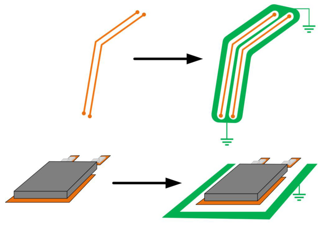
    Figure 2: Guard rings can be used to minimize signal crosstalk. Source: Kinetic Technology.
  8. Designing Trace-to-Trace Separation

    Trace-to-trace separation is also overlooked in PCB design.Most designers are familiar with worldwide safety agency standards (UL, IEC, for example), which primarily address electrical hazards and flammability. However, these standards do not address reliability.A voltage potential between traces can cause metallic whiskers (dendrite) to grow over months or years. Eventually, the dendrite will short the traces and lead to product failure. PCB design standard IPC-2221, ‘Generic Standard on Printed Board Design,’ defines trace spacing requirements to avoid electromigration. Engineers should try to design the trace-to-trace distance to be above the IPC-2221 guidelines.

Taking the Preemptive Design Approach with Filtering

After all the PCB design guidelines, described above, have been observed, now it is time to apply the design strategy to include passive and active filtering to solve the EMI problem preemptively. Here are the pros and cons of each approach.

Passive EMI filtering

To minimize the impact of differential to common mode current conversion in the Ethernet interface design, a small CM inductor, commonly known as balun, can be added. The transformer action (assuming a coupling coefficient of 1.00 and ignoring magnetizing current), of the CM inductor will force the currents in each line of the differential pair to be equal and opposite. The CM impedance is very high, and the differential impedance is (ideally) zero. To implement such a solution, the CM inductor is placed as part of the layout. Upon the final test, if it is not needed, it can be removed from the bill of materials (BOM) and replaced with a jumper.

However, a passive filter solution can cause performance to degrade in some applications. The degradation occurs because CM inductors do not have an ideal zero differential impedance, so there is an introduction of insertion loss and characteristic impedance.

Active EMI Filtering

Alternatively, active filtering can be implemented to solve the EMI problem. During the final test cycle, if the PWB design already meets EMC, then there is no need to install the active filter. Otherwise, include the active components in the PWB. This can be done by creating a placeholder on the PCB and calling this out in the BOM as an option.

Here is how active filtering works. As shown in Figure 3, either the dual-channel (KTA1550) or the quad-channel (KTA1552) active EMI & electrostatic discharge (ESD) suppressor IC from Kinetic for Ethernet applications can be routed through the data lines as a contingency. The IC is located between the PHY and the LAN transformer.

The KTA1550 supports two twisted pairs (Figure 4) while the KTA1552 supports four. Active filtering reduces the noise level via common mode rejection. If passive filtering is already installed, the add-on active filtering functions can achieve additional noise reduction.
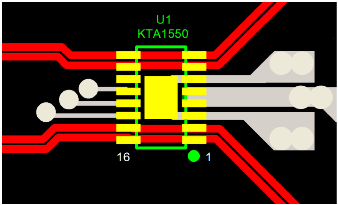
Figure 3: An active filter may route through the data lines. Source: Kinetic Technology.
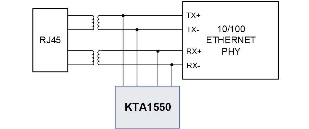
Figure 4: The dual-channel Kinetic KTA1550 active filtering IC is shown connected to the Ethernet data lines. Source: Kinetic Technology.

Using active filtering can reduce CM emissions by up to 10dB from 1 to 125MHz with almost no impact to insertion, return loss, or characteristic impedance compared with the passive-only approach. Both ICs are compatible with voltage and current mode PHYs. Operating in the Industrial temperature range from -40°C to +85°C, the device consumes 180mW with a single standard power rail (3.3V or 2.5V).

Common applications of active filters include Ethernet systems requiring additional CM suppression to meet EMC Class B emissions or higher EMI immunity requirements and ESD protection, PoE and non-PoE Ethernet systems, VoIP phones, IP cameras, and other network installations.

An active filter IC will have higher BOM costs than a passive balun, but the active filter IC is more successful at lowering noise, as Figures 5 through 7 indicate. The benefits of using active filter can be summarized as follow.

  • Higher common mode rejection can be achieved than using passive filtering alone.
  • No insertion loss or introduction of characteristic impedance compared with passive filtering.
  • Additional ESD suppression will come from the active filter IC
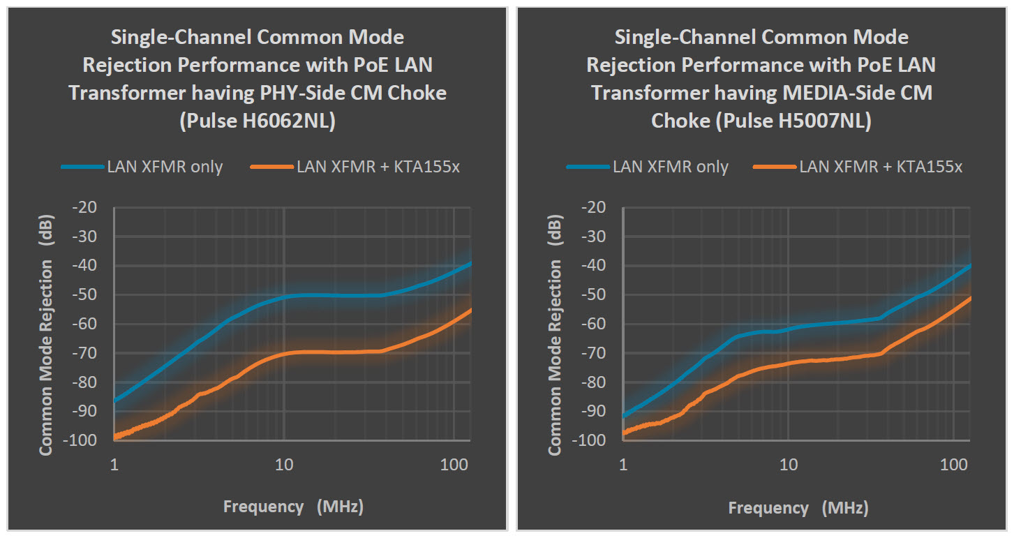
Figure 5: An active filter can significantly reduce the noise level by working with different configurations of passive filtering (PHY side CM choke, left; MEDIA side CM choke, right). Source: Kinetic Technology.
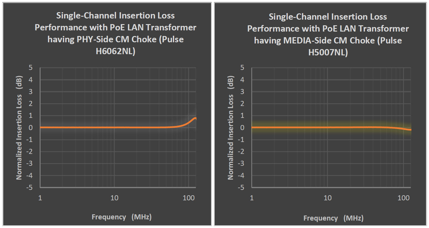
Figure 6: Using with PHY-side CM choke (left) or MEDIA-side CM choke (right), an active filter causes minimal insertion loss. Source: Kinetic Technology.
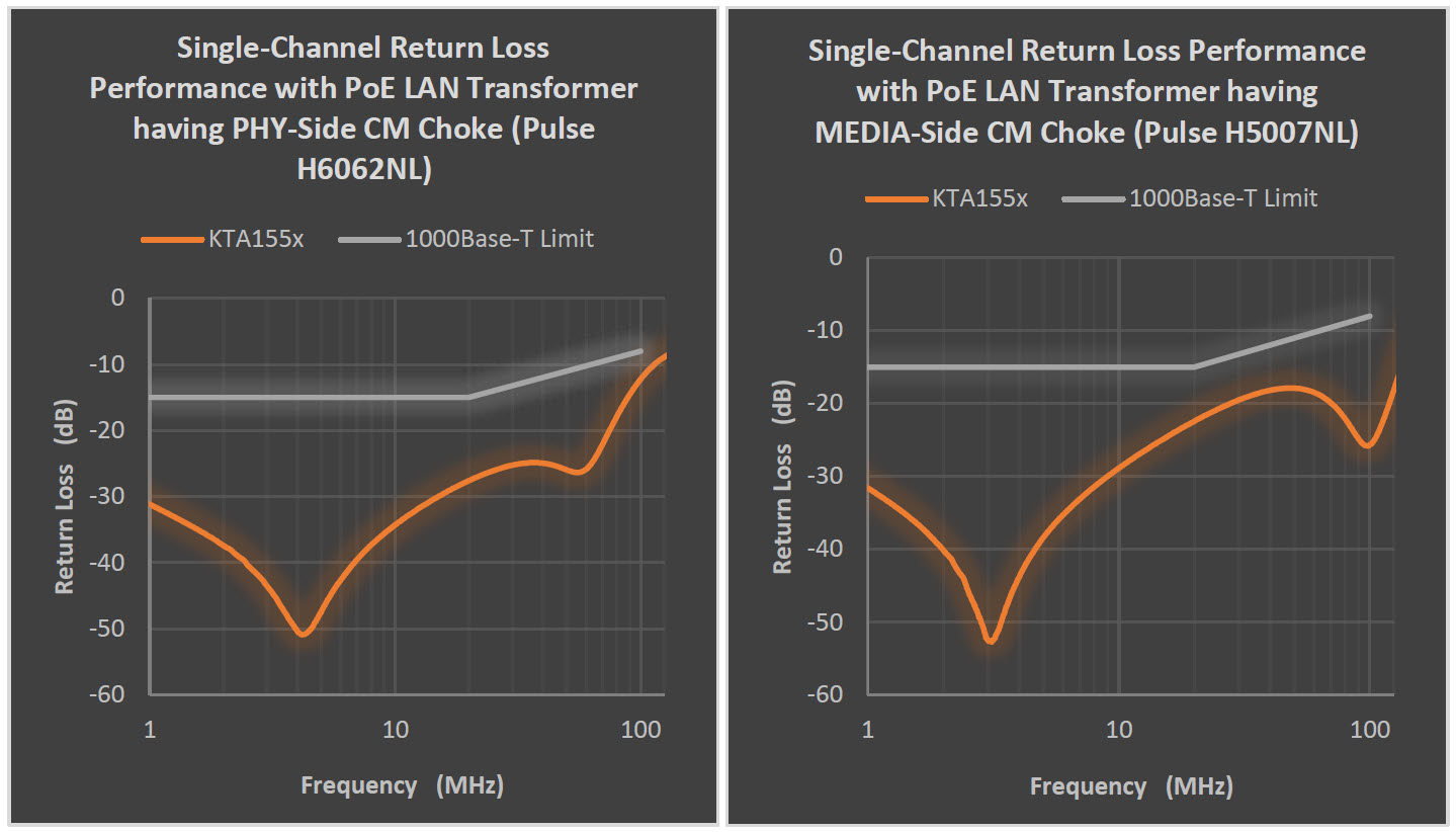
Figure 7: An active filter reduces return Loss more than other transformer configurations: PHY-side CM choke (left) or MEDIA-side CM choke (right). Source: Kinetic Technology.

Summary

Electromagnetic interference is a serious issue in printed wiring boards (PWB). Therefore, the reduction of EMI-induced noise is a significant challenge in PCB design.

Engineers often get trapped in a whack-a-mole scenario, where they have to keep adjusting the design to address new problems that arise from attempts to solve old issues. As a result, the PCB design has to undergo many rounds of redesign and re-testing, causing production delays and incurring extra development costs.

Active filters can help engineers solve this conundrum by achieving complete noise suppression without creating new noise-related issues. Furthermore, active filters fit easily into PCB designs and are equally easy to install. Therefore, they provide a significant return on investment, reducing design and production delays, and minimizing costs.

For more details on PCB design rules download the white paper here.


About Kinetic Technologies

Kinetic Technologies designs, develops and markets proprietary high-performance analog and mixed-signal power and protection semiconductors across consumer, communications, industrial, automotive and enterprise markets, to deliver protected solutions tolerant of real-world fault conditions. The company’s product sit “Behind Every Port™”, deliver solutions to not only provide, protect, regulate, and monitor power consumed by analog and digital semiconductors and other electronic loads, but to also switch, transform and protect high resolution video, audio and data signals. Kinetic Technologies develops application-specific products that solve audio-video interface, protection, and power management needs across smartphones, tablets and wearables, as well as serving a wide range of industrial, automotive and enterprise solutions. Kinetic Technologies, a Cayman Corporation, has R&D centers in Silicon Valley and Asia, with operations and logistics based in Asia. For more information, please visit http://www.kinet-ic.cn/.

*The Kinetic Technologies logo is a trademark of Kinetic Technologies. All other brand and product names appearing in this document are the property of their respective holders.

New LCD Power Solution from Kinetic Technologies Increases Performance and Reduces Overall Size by 32 Percent

KTZ8864: High Efficiency 4-channel LED Backlight Driver with Dual Output LCD Bias Power

San Jose, Calif. – July 29, 2019 – Power management leader, Kinetic Technologies, is expanding its Display Power portfolio with the introduction of KTZ8864, a high efficiency, 4- channel, step-up LED driver with dual output LCD bias power. Designed specifically for small to medium sized LCD panels, the KTZ8864 offers higher efficiency and more programmability than competitors’ discrete solutions—and in a smaller package that offers more than 32 percent savings in board space.

Senior Director of Mobile in the Kinetic Technologies Marketing group, Erik Ogren, says, “This is the latest addition to our extensive Display Power portfolio which continues our focus on highly integrated solutions with a reduced footprint and added value. The KTZ8864 combines the two main power functions required by the LCD panel, namely the multi-channel LED backlight driver and the LCD panel bias, all controlled from a single I2C compatible interface providing our customers with a high efficiency solution that has a multitude of flexible programable configuration options, all within a compact 1.72mm x 2.45mm package.”

The 4-channel LED backlight driver features a step-up converter with an integrated 35V low side power MOSFET, achieving a peak efficiency of 87 percent. The LED current in each channel can be programmed via the I2C compatible interface in 2047-steps (linear or exponential steps) or via the PWM-dimming input, which achieves high accuracy across a wide dimming range and can go down to an impressive 0.2 percent duty cycle at 20kHz. Super-wide dimming range allows programming down to 60µA with steps as low as 0.15µA. Auto-frequency mode automatically adjusts the converter switching frequency to maximize the efficiency for the programmed output current.

The LCD bias driver section uses a single inductor and can support up to 120mA from each of the outputs, with peak efficiency up to 85 percent. The positive and negative voltage outputs and turn-on sequence are configurable via the I2C compatible interface. Output voltages from +/- 4.0V to +/-6.3V can be programmed in 50mV steps, while the turn-on sequence can also be manually controlled.

Key applications for the new KTZ8864 include LCD bias and backlight LED drivers, which reach across smartphones, tablets, camcorders, digital cameras and more.

KTZ8864 is available and shipping now. Visit Kinetic Technologies for more information.

Product features include:

  • Pb-free Package: WLCSP-24 1.72×2.45mm
  • LED Backlight Driver
    • 4-Ch Current Sinks
      • Drives up to 8 series LEDs
      • Up to 30mA per channel
    • Backlight efficiency: up to 87 percent
    • Flexible dimming control
      • 2047-step(11 bits) I2C compatible control or
      • Programming down to 60µA with steps as low as 0.15µA
      • PWM dimming frequency 100Hz~100kHz, supporting 0.2 percent duty @ 20kHz
    • 3 bit programmable internal over voltage protection (default 21.0V)
  • LCD Bias Supplies
    • LCD bias efficiency: up to 85 percent
    • Wide dual output voltage range
      • Programmable +/-4.0V to +/-6.3V (50mV/step)
      • Output current up to 120mA
    • Programmable supply sequencing


About Kinetic Technologies

Kinetic Technologies designs, develops and markets proprietary high-performance analog and mixed-signal power and protection semiconductors across consumer, communications, industrial, automotive and enterprise markets, to deliver protected solutions tolerant of real-world fault conditions. The company’s product sit “Behind Every Port™”, deliver solutions to not only provide, protect, regulate, and monitor power consumed by analog and digital semiconductors and other electronic loads, but to also switch, transform and protect high resolution video, audio and data signals. Kinetic Technologies develops application-specific products that solve audio-video interface, protection, and power management needs across smartphones, tablets and wearables, as well as serving a wide range of industrial, automotive and enterprise solutions. Kinetic Technologies, a Cayman Corporation, has R&D centers in Silicon Valley and Asia, with operations and logistics based in Asia. For more information, please visit http://www.kinet-ic.cn/.

*The Kinetic Technologies logo is a trademark of Kinetic Technologies. All other brand and product names appearing in this document are the property of their respective holders.

Join Kinetic Technologies at MWC 2019 for a Preview of Leading Mobile Power Management and Wireless Charging Solutions

An invitation: Meet with Kinetic Technologies at MWC 2019, Barcelona, for a first-hand look at the power management leader’s mobile solutions

San Jose, Calif. – February 19, 2019 – Silicon Valley-based Kinetic Technologies will land in Barcelona, Spain, from February 25 to 28, for Mobile World Congress (MWC) 2019 to showcase its leading, mobile-focused power management solutions.

Leadership and engineering teams will be on site at MWC to walk through product demonstrations and end-application teardowns that highlight Kinetic’s mobile and internet of things (IoT) solutions, including:

  • Wireless Charging
  • USB Type-C
  • Display Power
  • Overvoltage Protection

Kinetic will also feature RGB LED driver and display power system product demonstrations and competitor comparisons.

MWC attendees are invited to stop by Kinetic’s meeting room at the Fira Gran Via conference center (Hall 5, room 5L36MR) to meet with company leadership and engineering teams. Appointments are also available—simply email info@kinet-ic.com to schedule time.

MWC 2019 Kinetic Technologies event details:

  • When: Monday, February 25 through Thursday, February 28
  • Where: Barcelona, Spain—Fira Gran Via conference center, Hall 5, room 5L36MR
  • Stop by, or schedule a meeting: Email info@kinet-ic.com to schedule time with the Kinetic team


About Kinetic Technologies

Kinetic Technologies designs, develops and markets proprietary high-performance analog and mixed-signal power and protection semiconductors across consumer, communications, industrial, automotive and enterprise markets, to deliver protected solutions tolerant of real-world fault conditions. The company’s product sit “Behind Every Port™”, deliver solutions to not only provide, protect, regulate, and monitor power consumed by analog and digital semiconductors and other electronic loads, but to also switch, transform and protect high resolution video, audio and data signals. Kinetic Technologies develops application-specific products that solve audio-video interface, protection, and power management needs across smartphones, tablets and wearables, as well as serving a wide range of industrial, automotive and enterprise solutions. Kinetic Technologies, a Cayman Corporation, has R&D centers in Silicon Valley and Asia, with operations and logistics based in Asia. For more information, please visit http://www.kinet-ic.cn/.

*The Kinetic Technologies logo is a trademark of Kinetic Technologies. All other brand and product names appearing in this document are the property of their respective holders.

Kinetic Technologies’ Latest Device Isolates and Protects Against Abnormal Voltage and Current Conditions

KTS1677A: Low RON Load Switch with Overvoltage and Reverse Blocking, Protects Against ±90V Input Surges

San Jose, Calif. – February 7, 2019 – Power management leader Kinetic Technologies has announced a new addition to their ever-growing power protection solutions with the KTS1677A. This innovative protection device has been designed to isolate and protect against abnormal voltage and current conditions through a slew-rate controlled, reverse-blocking, 30mΩ, low-resistance MOSFET switch.

“In addition to its ability to protect USB inputs from abnormal power supply voltage and surge currents, the KTS1677A features reverse-blocking capability up to 30V.” says David Nam, Vice President of Kinetic Technologies. “This allows two devices, used in a Power OR configuration to support dual USB inputs connecting to a single system.

In addition to the low-resistance MOSFET switch, the KTS1677A features slew-rate turn-on control, preventing excessive voltage overshoot and large inrush currents. The device also features several additional protection functions – including input ±90V surge protection, input over – and under – voltage protection, and over-temperature protection. The over-voltage protection is internally set at typically 23V but can also be used in adjustable mode using two external resistors to set the trip point between 4V and  23V.

The KTS1677A operates via a wide-input voltage range of 3V to 30V and covers USB PD applications, enabling the device to offer essential protection to enhancing system reliability.

The KTS1677A is available in a green compliant, 2.57mm x 1.57mm, Wafer-Level, Chip-Scale Package (WLCSP).

Key applications for the Kinetic Technologies KTS1677A include computers, tablets, mobile internet devices, storage, DLSR, portable devices and USB Type-C power source switches.

The KTS1677A is available and shipping now. Visit Kinetic Technologies for more information.


About Kinetic Technologies

Kinetic Technologies designs, develops and markets proprietary high-performance analog and mixed-signal power and protection semiconductors across consumer, communications, industrial, automotive and enterprise markets, to deliver protected solutions tolerant of real-world fault conditions. The company’s product sit “Behind Every Port™”, deliver solutions to not only provide, protect, regulate, and monitor power consumed by analog and digital semiconductors and other electronic loads, but to also switch, transform and protect high resolution video, audio and data signals. Kinetic Technologies develops application-specific products that solve audio-video interface, protection, and power management needs across smartphones, tablets and wearables, as well as serving a wide range of industrial, automotive and enterprise solutions. Kinetic Technologies, a Cayman Corporation, has R&D centers in Silicon Valley and Asia, with operations and logistics based in Asia. For more information, please visit http://www.kinet-ic.cn/.

*The Kinetic Technologies logo is a trademark of Kinetic Technologies. All other brand and product names appearing in this document are the property of their respective holders.